Please wait...
After Rajendra Chola returned from his voyage to Indonesia, he _______ to visit the temple in Thanjavur.
Find the smallest number y such that y × 162 is a perfect cube.
“The hold of the nationalist imagination on our colonial past is such that anything inadequately or improperly nationalist is just not history.”
Which of the following statements best reflects the author’s opinion?
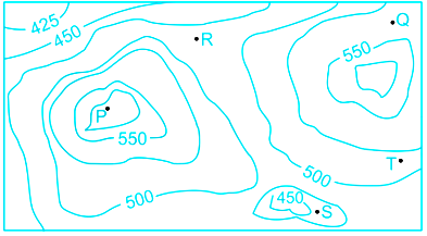
A contour line joins locations having the same height above the mean sea level. The following is a contour plot of a geographical region. Contour lines are shown at 25m intervals in this plot. If in a flood, the water level rises to 525m. Which of the villages P, Q, R, S, T get submerged?
The transfer function of a system is given by,
\(\frac{{{V_0}\left( s \right)}}{{{V_i}\left( s \right)}} = \frac{{1 - s}}{{1 + s}}\)
Consider the system with following input-output relation
\(y\left[ n \right] = \left[ {1 + {{\left( { - 1} \right)}^n}} \right]x\left[ n \right]\)
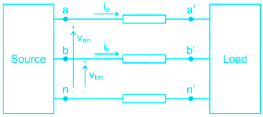
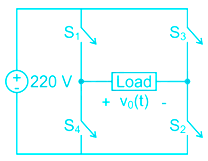
A source is supplying a load through a 2-phase, 3-wire transmission system as shown in figure below. The instantaneous voltage and current in phase-a are \({V_{an}} = 220\sin \left( {100\pi t} \right)V\) and \({i_a} = 10\sin \left( {100\pi t} \right)A\) respectively. Similarly, for phase-b, the instantaneous voltage and current are \({V_{bn}} = 220\cos \left( {100\pi t} \right)V\) and \({i_b} = 10\cos \left( {100\pi t} \right)A\) respectively.
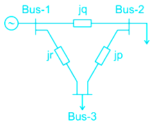
A 3-bus power system is shown in the figure below, where the diagonal elements of Y-bus matrix are: Y11 = -j12 pu, Y22 = -j15 pu and Y33 = -j7 pu.
The per unit values of the line reactances p, q and r shown in the figure are
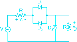
For the circuit shown in the figure below, assume that D1, D2 and D3 are ideal. v(t) = π sin (100πt) V
The DC components of voltages v1 and v2, respectively are
Consider \(g\left( t \right) = \left\{ {\begin{array}{*{}{}} {t - {{\lfloor}t{\rfloor}},\;\;t \ge 0}\\ {t - {\lceil}t{\rceil},\;\;otherwise} \end{array}} \right.\), where t ϵ R.
Here, \({\lfloor}t{\rfloor}\) represents the largest integer less than or equal to t and \({\lceil}t{\rceil}\) denotes the smallest integer greater than or equal to t. The coefficient of the second harmonic component of the Fourier series representing g(t) is ________
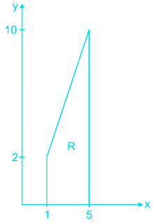
Let \(I = c\mathop \int\!\!\!\int \limits_R x{y^2}dx\;dy\), where R is the region shown in the figure and c = 6 × 10⁻⁴. The value of I equals________. (Give the answer up to two decimal places.)
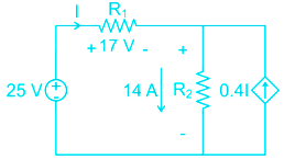
The power supplied by the 25 V source in the figure shown below is ________ W.
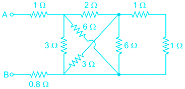
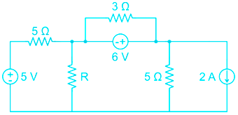
The equivalent resistance between the terminals A and B is ________ Ω.
Consider the unity feedback control system shown. The value of K that results in a phase margin of the system to be 30° is __________. (Give the answer up to two decimal places.)
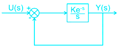
In the converter circuit shown below, the switches are controlled such that the load voltage v0(t) is a 400 Hz square wave.
The RMS value of the fundamental component of v0(t) in volts is _________.
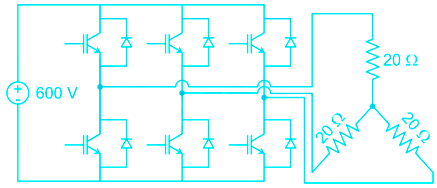
A 3-phase voltage source inverter is supplied from a 600 V DC source as shown in the figure below. For a star connected resistive load of 20 Ω per phase, the load power for 120° device conduction, in kW, is ____________.
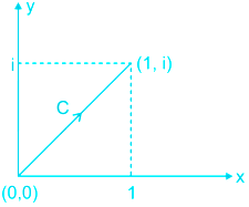
Consider the line integral \(I = \mathop \smallint \limits_C \left( {{x^2} + i{y^2}} \right)dz\), where z = x + iy. The line C is shown in figure below.
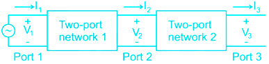
Two passive two-port networks are connected in cascade as shown in figure. A voltage source is connected at port 1.
Given V1 = A1V2 + B1I2
I1 = C1V2 + D1I2
V2 = A2V3 + B2I3
I2 = C2V3 + D2I3
A1, B1, C1, D1, A2, B2, C2, and D2 are the generalized circuit constants. If the Thevenin equivalent circuit at port 3 consists of a voltage source VT and an impedance ZT connected in series, then
Let a causal LTI system be characterized by the following differential equation, with initial rest condition
\(\frac{{{d^2}y}}{{d{t^2}}} + 7\frac{{dy}}{{dt}} + 10y\left( t \right) = 4x\left( t \right) + 5\frac{{dx\left( t \right)}}{{dt}}\)
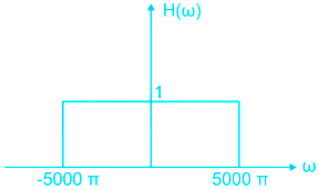
Let the signal \(x\left( t \right) = \mathop \sum \limits_{k = - \infty }^{ + \infty } {\left( { - 1} \right)^k}\delta \left( {t - \frac{k}{{2000}}} \right)\) be passed through an LTI system with frequency response H(ω), as given in the figure below.
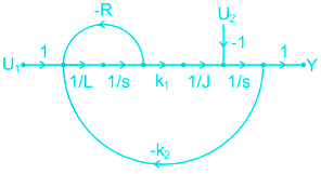
In the system whose signal flow graph is shown in the figure, U1(s) and U2(s) are inputs. The transfer function \(\frac{{Y\left( s \right)}}{{{U_1}\left( s \right)}}\) is
The transfer function of the system \(\frac{{Y\left( s \right)}}{{U\left( s \right)}}\) whose state-space equations are given below is:
\(\left[ {\begin{array}{*{20}{c}}{{{\dot x}_1}\left( t \right)}\\{{{\dot x}_2}\left( t \right)}\end{array}} \right] = \left[ {\begin{array}{*{20}{c}}1&2\\2&0\end{array}} \right]\left[ {\begin{array}{*{20}{c}}{{x_1}\left( t \right)}\\{{x_2}\left( t \right)}\end{array}} \right] + \left[ {\begin{array}{*{20}{c}}1\\2\end{array}} \right]u\left( t \right)\)
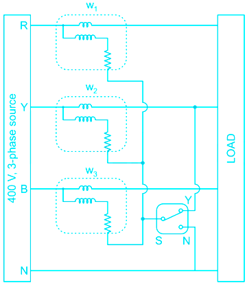
The load shown in the figure is supplied by a 400 V (line-to-line), 3-phase source (RYB sequence). The load is balanced and inductive, drawing 3464 VA. When the switch S is in position N, the three wattmeters W1, W2 and W3 read 577.35 W each. If the switch is moved to position Y, the readings of the wattmeters in watts will be:
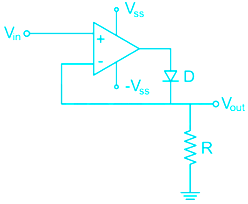
The approximate transfer characteristic for the circuit shown below with an ideal operational amplifier and diode will be
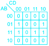
The output expression for the Karnaugh map shown below is:
The logical gate implemented using the circuit shown below where, V1 and V2 are inputs (with 0 V as digital 0 and 5 V as digital 1) and VOUT is the output, is
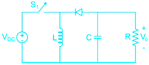
The input voltage VDC of the buck-boost converter shown below varies from 32 V to 72 V. Assume that all components are ideal, inductor current is continuous, and output voltage is ripple free. The range of duty ratio D of the converter for which the magnitude of the steady-state output voltage remains constant at 48 V is
The bus admittance matrix for a power system network is
\(\left[ {\begin{array}{*{20}{c}}{ - j39.9}&{j20}&{j20}\\{j20}&{ - j39.9}&{j20}\\{j20}&{j20}&{ - j39.9}\end{array}} \right]pu\)
There is a transmission line, connected between buses 1 and 3, which is represented by the circuit shown in figure.
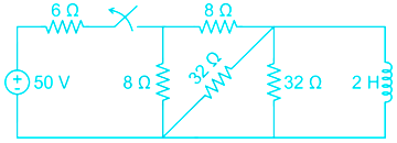
The switch in the below figure was closed for a long time. It is opened at t = 0. The current in the inductor of 2 H for t ≥ 0, is
In the circuit shown below, the maximum power transferred to the resistor R is ________ W.
The magnitude of magnetic flux density (B) in micro Teslas (μT), at the centre of a loop of wire wound as a regular hexagon of side length 1 m carrying a current (I = 1 A ) and placed in vacuum as shown in the figure is __________. (Give the answer up to two decimal places.)
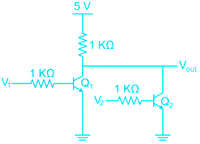
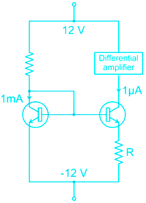
The circuit shown in the figure uses matched transistors with a thermal voltage VT = 25 mV. The base currents of the transistors are negligible. The value of the resistance R in kΩ that is required to provide 1 μA bias current for the differential amplifier block shown is ___________. (Give the answer up to one decimal place.)
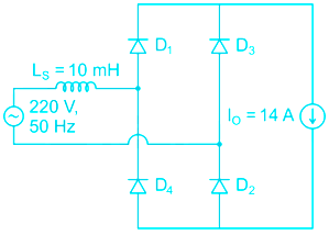
The figure below shows an uncontrolled diode bridge rectifier supplied from a 220 V, 50 Hz, 1-phase ac source. The load draws a constant current I0 = 14 A. The conduction angle of the diode D1 in degrees (rounded off to two decimal places) is ________.
The figure shows the single line diagram of a power system with a double circuit transmission line. The expression for electrical power is 1.5 sin δ, where δ is the rotor angle. The system is operating at the stable equilibrium point with mechanical power equal to 1 pu. If one of the transmission line circuits is removed, the maximum value of δ, as the rotor swings, is 1.221 radian. If the expression for electrical power with one transmission line circuit removed is Pmax sin δ, the value of Pmax, in pu is ______. (Give the answer up to three decimal places.)


 ×
×
 Bank
Bank


 SSC
SSC


 Railway


 State
State


 Other
Other


 Teaching


 Insurance


 Medical


 Engineering


 Defence


 GATE
GATE


 NTA CUET

 UPSC
UPSC

 MBA Entrance


 LAW
LAW

 JEE Advanced 2026
 CUET UG 2026
 NEET UG 2026
 UP Police Constable 2026
 SSC Selection Post (Phase 14) 2026
 SSC GD 2025-26
 RRB NTPC 2026
 SSC CGL Tier-I 2026
 SSC JE 2026
 UPSC (CSE) 2026
 SBI PO Prelims 2026
 SSC Steno Grade C & D 2026