Please wait...
An apple costs Rs. 10. An onion costs Rs. 8.
Select the most suitable sentence with respect to grammar and usage.
The Buddha said, “Holding on to anger is like grasping a hot coal with the intent of throwing it at someone else; you are the one who gets burnt.”
Select the word below which is closest in meaning to the word underlined above.
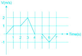
The velocity V of a vehicle along a straight line is measured in m/s and plotted as shown with respect to time in seconds. At the end of the 7 seconds, how much will the odometer reading increase by (in m)?
The overwhelming number of people infected with rabies in India has been flagged by the world Health Organization as a source of concern. It is estimated that inoculating 70% of pets and stray dogs against rabies can lead to a significant reduction in the number of people infected with rabies.
Which of the following can be logically inferred from the above sentences?
Consider a 2 × 2 square matrix.
\({\rm{A}} = \left[ {\begin{array}{*{20}{c}} {\rm{\sigma }}&{\rm{x}}\\ {\rm{\omega }}&{\rm{\sigma }} \end{array}} \right]\)
Consider the first order initial value problem
y' = y + 2x − x2, y(0) = 1, (0 ≤ x < ∞)
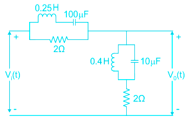
In the RLC circuit shown in the figure, the input voltage is given by vi(t) = 2cos (200t) + 4 sin (500t). The output voltage v0(t) is:
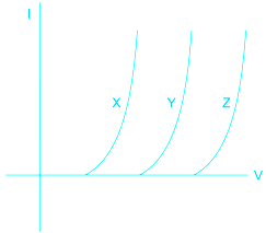
The I-V characteristics of three types of diodes at room temperature made of semiconductors X, Y, and Z, are shown in the figure. Assume that the diodes are uniformly doped and identical in all respects except their materials. If EgX, EgY, and EgZ are the band gaps of X, Y, and Z, respectively, then
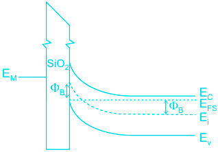
The figure shows the band diagram of a Metal Oxide Semiconductor (MOS). The surface region of this MOS is in
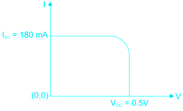
The figure shows the I-V characteristics of a solar cell illuminated uniformly with solar light of power 100 mW/cm2. The solar cell has an area of 3 cm2 and a fill factor of 0.7. The maximum efficiency (in %) of the device is __________
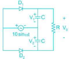
The diodes D1 and D2 in the figure are ideal and the capacitors are identical. The product RC is very large compared to the time period of the ac voltage. Assuming that the diodes do not breakdown in the reverse bias, the output voltage VO (in volt) at the steady-state is ______.
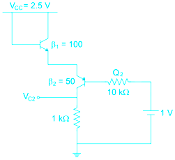
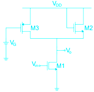
Consider the circuit shown in the figure. Assuming VBE1 = VEB2 = 0.7 volt, the value of the dc voltage VC2 (in volt) is __________
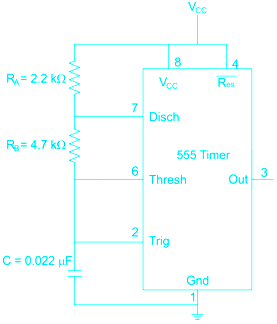
In the astable multivibrator circuit shown in the figure, the frequency of oscillation (in kHz) at the output pin 3 is __________
The logic functionality realized by the circuit shown below is
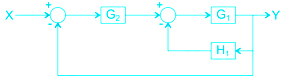
The block diagram of a feedback control system is shown in the figure. The overall closed – loop gain G of the system is
For the unity feedback control system shown in the figure, the open-loop transfer function G(s) is given as
\({\rm{G}}\left( {\rm{s}} \right) = \frac{2}{{{\rm{s}}\left( {{\rm{s}} + 1} \right)}}\)
The steady-state error ess due to a unit step input is
A binary baseband digital communication system employs the signal
\({\rm{p}}\left( {\rm{t}} \right) = \left\{ {\begin{array}{*{20}{c}} {\frac{1}{{\sqrt {{{\rm{T}}_{\rm{s}}}} }},}&{0 \le {\rm{t}} \le {{\rm{T}}_{\rm{s}}}}\\ {0,}&{{\rm{otherwise}}} \end{array}} \right.{\rm{\;}}\)
If a right-handed circularly polarized wave is incident normally on a plane perfect conductor, then the reflected wave will be
The particular solution of the initial value problem given below is:
\(\frac{d^2y}{dx^2}+12\frac{dy}{dx}+36y=0\), with y = 3 and \(\frac{dy}{dx}|_{x=0}=-36\)
The values of the integral \(\frac{1}{{2{\rm{\pi j}}}}\mathop \oint \limits_{\rm{c}} \frac{{{{\rm{e}}^{\rm{z}}}}}{{{\rm{z}} - 2}}{\rm{\;}}\)along a closed contour c in anti-clockwise direction for
(i) the point z0 = 2 inside the contour c, and
A signal \(2\cos \left( {\frac{{2{\rm{\pi }}}}{3}{\rm{t}}} \right) - {\rm{cos}}\left( {{\rm{\pi t}}} \right){\rm{\;}}\)is input to an LTI system with the transfer function
H(s) = es + e-s
If ck denotes the kth coefficient in the exponential Fourier series of the output signal, then c3 is equal to
Assume that the circuit in the figure has reached the steady state before time 𝑡 = 0 when the 3 Ω resistor suddenly burns out, resulting in an open circuit. The current (𝑡) (in ampere) at 𝑡 = 0+ is __________
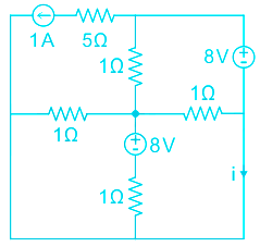
In the figure shown, the current 𝑖 (in ampere) is __________
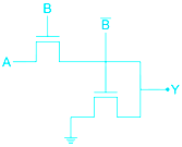
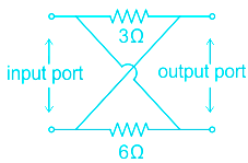
The z-parameter matrix \(\left[ {\begin{array}{*{20}{c}} {{{\rm{z}}_{11}}}&{{{\rm{z}}_{12}}}\\ {{{\rm{z}}_{21}}}&{{{\rm{z}}_{21}}} \end{array}} \right]{\rm{}}\) for the two-port network shown is.
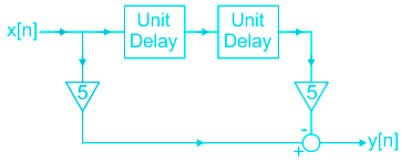
The direct form structure of an FIR (finite impulse response) filter is shown in the figure:
The filter can be used to approximate a
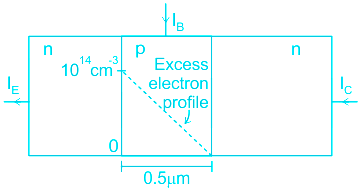
The injected excess electron concentration profile in the base region of an npn BJT, biased in the active region, is linear, as shown in the figure. If the area of the emitter-base junction is 0.001 cm2, μn = 800 cm2/(V-s) in the base region and depletion layer widths are negligible, then the collector current IC (in mA) at room temperature is __________
(Given: thermal voltage VT = 26 mV at room temperature, electronic charge q = 1.6 × 10⁻¹⁹ C)
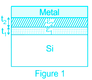
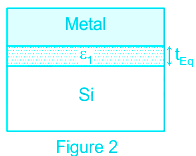
Figures I and II show two MOS capacitors of the unit area. The capacitor in Figure I has insulator materials X (of thickness t1 = 1 nm and dielectric constant ε1 = 4) and Y (of thickness t2 = 3 nm and dielectric constant ε2 = 20). The capacitor in Figure II has only insulator material X of thickness tEq. If the capacitors are of equal capacitance, then the value of tEq (in nm) is __________
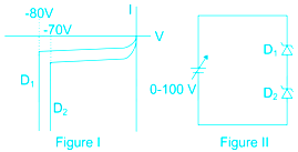
The I – V characteristics of the zener diodes D1 and D2 are shown in Figure I. These diodes are used in the circuit given in Figure II. If the supply voltage is varied from 0 to 100 V, then breakdown occurs in.
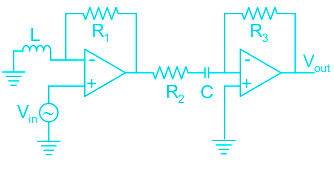
For the circuit shown in the figure, R1 = R2 = R3 = 1 Ω, L = 1 μH and C = 1 μF. If the input in Vin = cos(106t), then the overall voltage gain (Vout /Vin) of the circuit is __________.
In the circuit shown in the figure, the channel length modulation of all transistors is non-zero (λ ≠ 0). Also, all transistors operate in saturation and have negligible body effect. The ac small signal voltage gain (Vo/Vin) of the circuit is
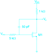
In the circuit shown in the figure, transistor M1 is in saturation and has transconductance gm = 0.01 siemens. Ignoring internal parasitic capacitances and assuming the channel length modulation λ to be zero, the small signal input pole frequency (in kHz) is __________
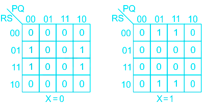
Following is the K-map of a Boolean function of five variables P, Q, R, S, and X. The minimum sum-of-product (SOP) expression for the function is
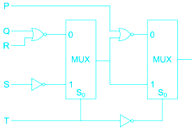
For the circuit shown in the figure, the delays of NOR gates, multiplexers and inverters are 2 ns, 1.5 ns and 1 ns, respectively. If all the inputs P, Q, R, S and T are applied at the same time instant, the maximum propagation delay (in ns) of the circuit is __________
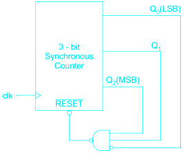
For the circuit shown in the figure, the delay of the bubbled NAND gate is 2 ns and that of the counter is assumed to be zero.
If the clock (Clk) frequency is 1 GHz, then the counter behaves as a
The first two rows in the Routh table for the characteristic equation of a certain closed-loop control system are given as
\({s^3}\)
1
(2K+3)
\({{\rm{s}}^2}\)
2K
4
The range of K for which the system is stable is
A second-order linear time-invariant system is described by the following state equations
\(\frac{{\rm{d}}}{{{\rm{dt}}}}{{\rm{x}}_1}\left( {\rm{t}} \right) + 2{{\rm{x}}_1}\left( {\rm{t}} \right) = 3{\rm{u}}\left( {\rm{t}} \right)\)
\( \frac{{\rm{d}}}{{{\rm{dt}}}}{{\rm{x}}_2}\left( {\rm{t}} \right) + {{\rm{x}}_2}\left( {\rm{t}} \right) = {\rm{u}}\left( {\rm{t}} \right) \)
where x1(t) and x2(t) are the two-state variables and u(t) denotes the input. If the output c(t) = x1(t), then the system is:
The forward-path transfer function and the feedback-path transfer function of a single loop negative feedback control system are given as
\({\rm{G}}\left( {\rm{s}} \right) = \frac{{{\rm{K}}\left( {{\rm{s}} + 2} \right)}}{{{{\rm{s}}^2} + 2{\rm{s}} + 2}}{~\rm{and\;H}}\left( {\rm{s}} \right) = 1\)
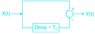
A wide sense stationary random process (𝑡) passes through the LTI system shown in the figure. If the autocorrelation function of (𝑡) is (𝜏), then the autocorrelation function (𝜏) of the output (𝑡) is equal to
The bit error probability of a memory less binary symmetric channel is 10−5. If 105 bits are sent over this channel, then the probability that not more than one bit will be in error is __________
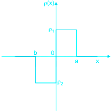
Consider the charge profile shown in the figure. The resultant potential distribution is best described by


 ×
×
 Bank
Bank


 SSC
SSC


 Railway


 State
State


 Other
Other


 Teaching


 Insurance


 Medical


 Engineering


 Defence


 GATE
GATE


 NTA CUET

 UPSC
UPSC

 MBA Entrance


 LAW
LAW

 ReNEET UG 2026
 CUET UG 2026
 UP Police Constable 2026
 SSC Selection Post (Phase 14) 2026
 SSC GD 2025-26
 RRB NTPC 2026
 SSC CGL Tier-I 2026
 SSC JE 2026
 UPSC (CSE) 2026
 SBI PO Prelims 2026
 SSC Steno Grade C & D 2026
 SBI Clerk Prelims 2026
 IBPS PO Prelims 2026
 IBPS Clerk Prelims 2026
 SSC CPO Tier I 2026