Please wait...
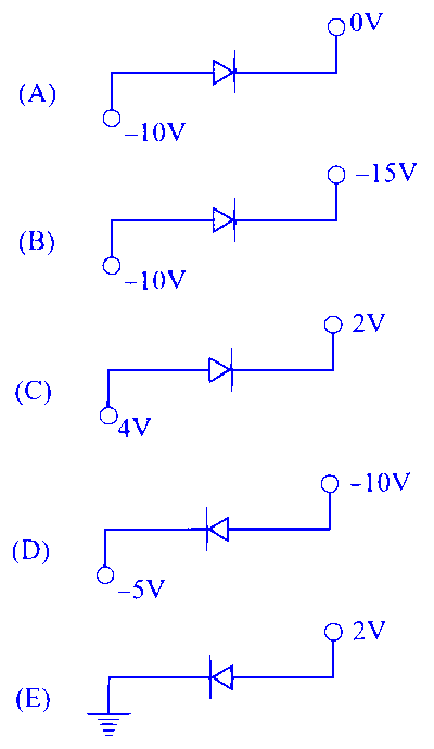
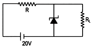
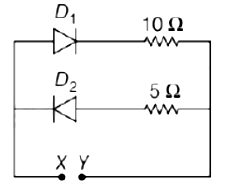
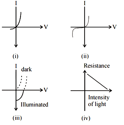
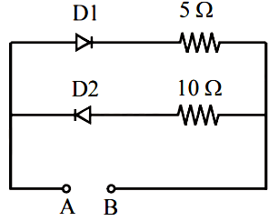
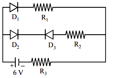
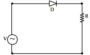
Which of the following circuits represents a forward biased diode?
Choose the correct answer from the options given below:
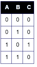
To obtain the given truth table, following logic gate should be placed at G :
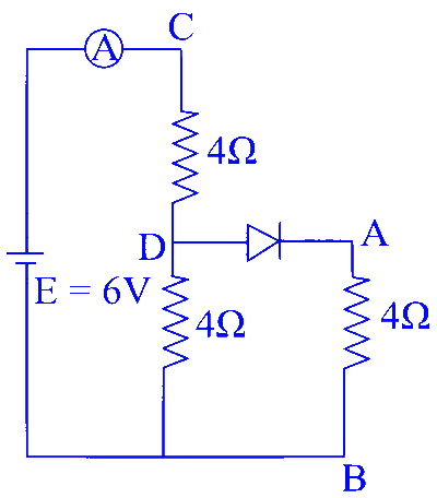
Refer to the circuit diagram given in the figure. which of the following observations are correct?
A. Total resistance of circuit is $6 \Omega$
B. Current in Ammeter is 1 A
C. Potential across $A B$ is 4 Volts.
D. Potential across CD is 4 Volts
E. Total resistance of the circuit is $8 \Omega$.
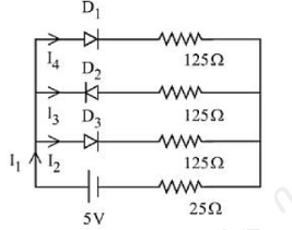
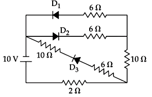
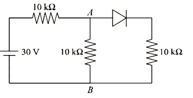
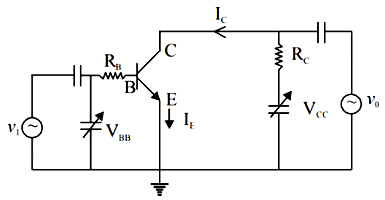
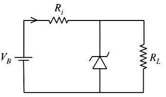
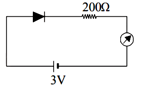
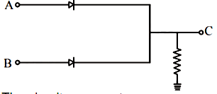
What is the current through the battery in the circuit shown below?
Consider the following statements :
A. The junction area of solar cell is made very narrow compared to a photo diode.
B. Solar cells are not connected with any external bias.
C. LED is made of lightly doped p-n junction.
D. Increase of forward current results in continuous increase of LED light intensity.
E. LEDs have to be connected in forward bias for emission of light.
Choose the correct answer from the options given below :
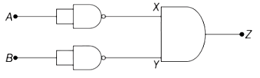
The output of the circuit is low (zero) for :
(A) $X=0, Y=0$
(B) $X=0, Y=1$
(C) $X=1, Y=0$
(D) $X=1, Y=1$
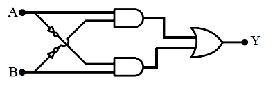
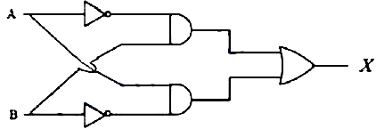
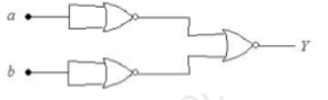
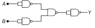
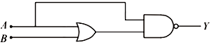
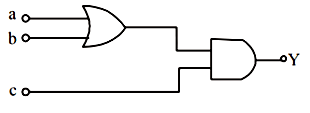
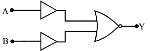
Which of the following circuits has the same output as that of the given circuit?
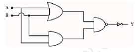
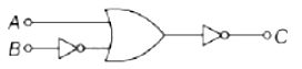
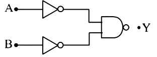
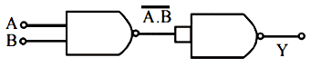
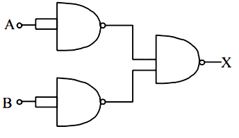
For the circuit shown above, equivalent GATE is :
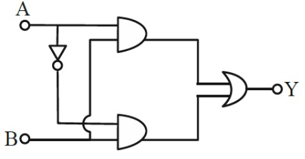
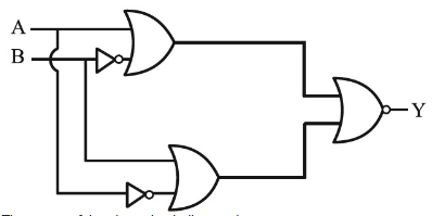
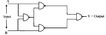
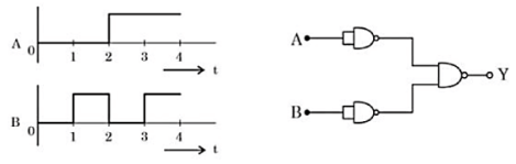
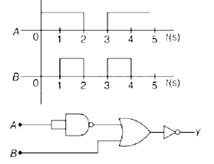
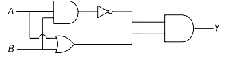
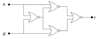
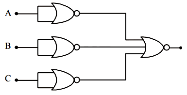
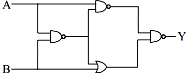
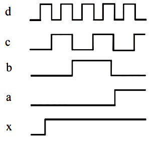
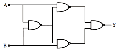
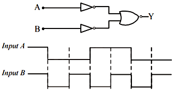
The truth table for the circuit given below is:
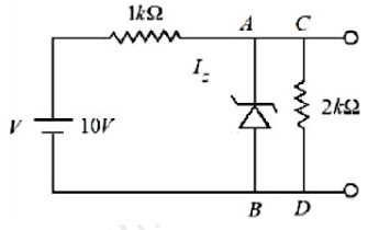
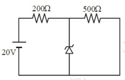
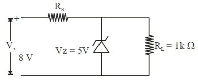
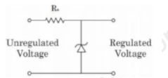
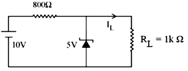
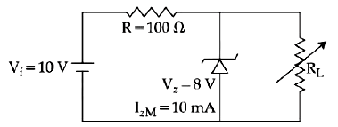
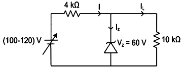
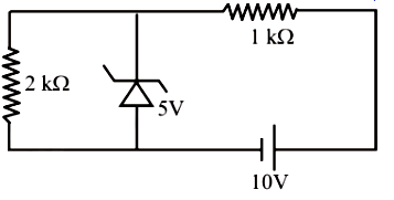
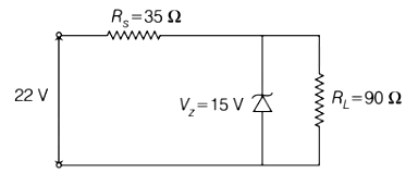
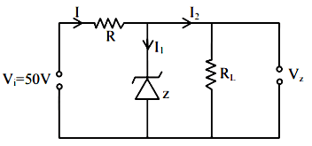
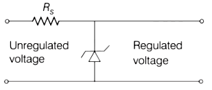
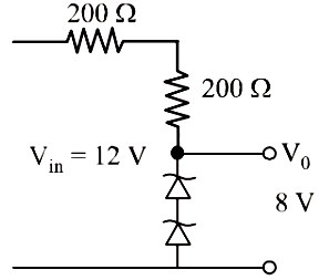
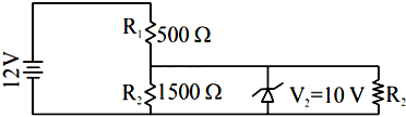
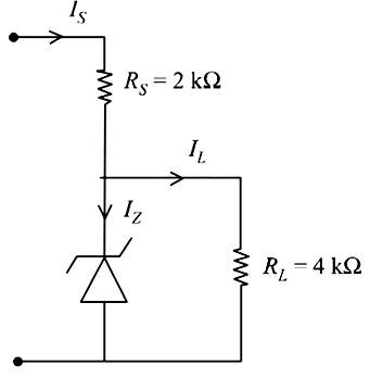
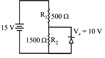
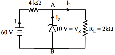
A zener diode with 5 V zener voltage is used to regulate an unregulated dc voltage input of 25 V . For a $400 \Omega$ resistor connected in series, the zener current is found to be 4 times load current. The load current $\left(I_L\right)$ and load resistance $\left(R_L\right)$ are :
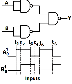
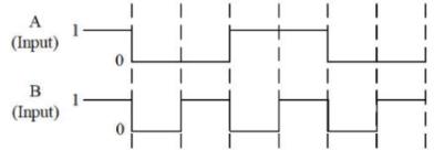
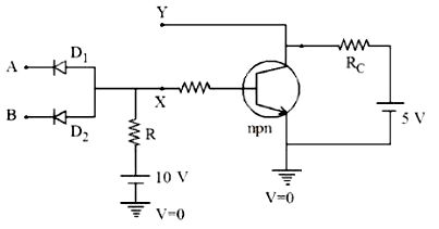
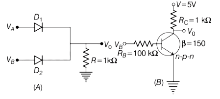
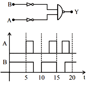
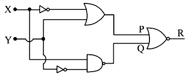
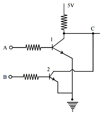
In the digital circuit shown in the figure, for the given inputs the P and Q values are :
JEE Main 2025 (Online) 2nd April Evening Shift
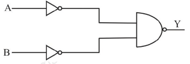
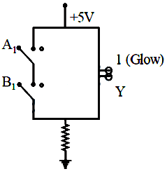
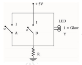
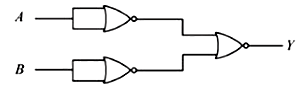
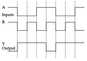
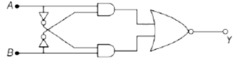
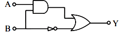
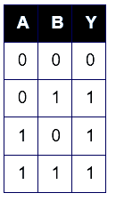
Choose the correct logic circuit for the given truth table having inputs A and B.
JEE Main 2025 (Online) 3rd April Morning Shift
$$ \text {The truth table corresponding to the circuit given below is: } $$
The Boolean expression $\mathrm{Y}=A \bar{B} C+\bar{A} \bar{C}$ can be realised with which of the following gate configurations.
A. One 3-input AND gate, 3 NOT gates and one 2-input OR gate, One 2-input AND gate,
B. One 3 -input AND gate, 1 NOT gate, One 2 -input NOR gate and one 2 -input OR gate
C. 3 -input OR gate, 3 NOT gates and one 2 -input AND gate
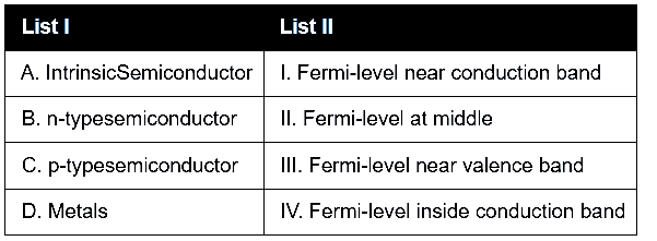
Consider a n-type semiconductor in which $\mathrm{n}_{\mathrm{e}}$ and $\mathrm{n}_{\mathrm{h}}$ are number of electrons and holes, respectively.
(A) Holes are minority carriers
(B) The dopant is a pentavalent atom
(C) $\mathrm{n}_{\mathrm{e}} \mathrm{n}_{\mathrm{h}} \neq \mathrm{n}_i^2$
(where $\mathrm{n}_i$ is number of electrons or holes in semiconductor when it is intrinsic form)
(D) $\mathrm{n}_{\mathrm{e}} \mathrm{n}_{\mathrm{h}} \geqslant \mathrm{n}_i^2$
(E) The holes are not generated due to the donors
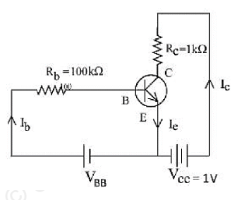
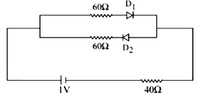
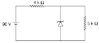
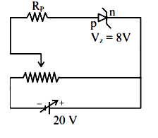
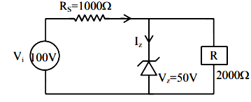
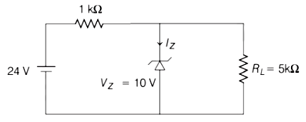
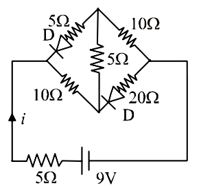
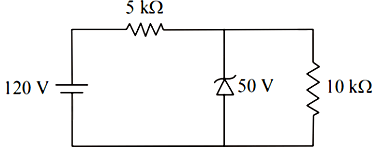
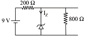
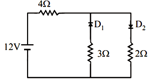
In the following circuit, the reading of the ammeter will be
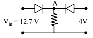
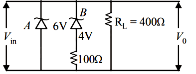
$($ Take Zener breakdown voltage $=4 \mathrm{~V})$
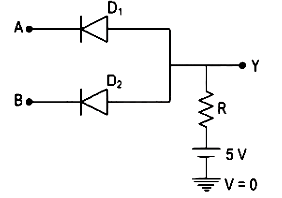
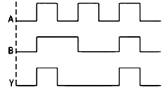
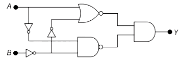
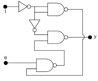
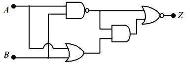
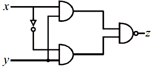
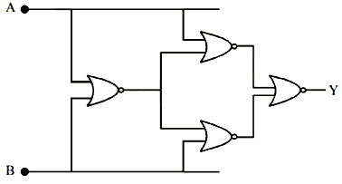
Consider the following logic circuit.
The output is Y = 0 when :
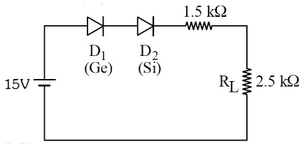
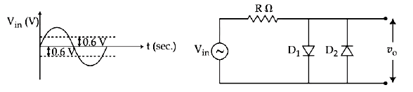
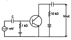
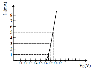
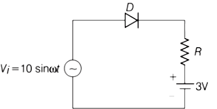
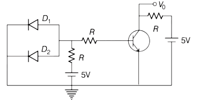
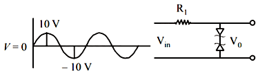
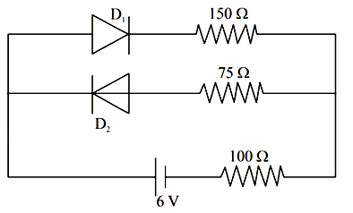
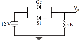
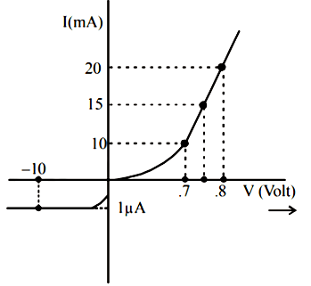
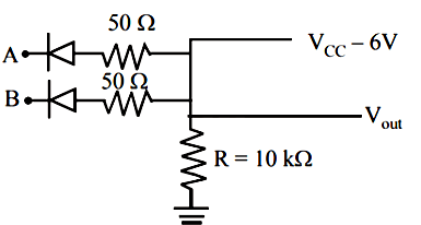
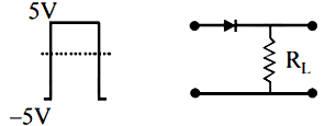
The output voltage in the following circuit is (Consider ideal diode case)


 ×
×
 Bank
Bank


 SSC
SSC


 Railway


 State
State


 Other
Other


 Teaching


 Insurance


 Medical


 Engineering


 Defence


 GATE
GATE


 NTA CUET

 UPSC
UPSC

 MBA Entrance


 LAW
LAW

 ReNEET UG 2026
 SSC Selection Post (Phase 14) 2026
 RRB NTPC 2026
 SSC CGL Tier-I 2026
 SSC JE 2026
 SBI PO Prelims 2026
 SSC Steno Grade C & D 2026
 SBI Clerk Prelims 2026
 IBPS PO Prelims 2026
 IBPS Clerk Prelims 2026
 SSC CPO Tier I 2026
 NDA II 2026
 CDS II 2026